Donn Stewart
13917 Deviar Dr
Centreville, VA 20120
dstew@cpuville.com
13917 Deviar Dr
Centreville, VA 20120
dstew@cpuville.com
The completed computer is shown below. The central three boards (ALU, main board and control) make up what is commonly thought of as a computer processor, or central processing unit (CPU). The processor takes instructions and data from the memory-input/output, processes them, and puts data back into the memory-input/output.
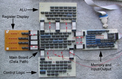
Each board is a separate functional unit. The four outside boards (ALU, display, control and memory) could be tested thoroughly using a simple test board before being connected to the central main board.
Before I built this computer, I had to design it. My priority was simplicity. I did not want a processor that was fast, or complex. I wanted it to work. This processor that I designed and built is an accumulator-memory machine, that is, a single register is used in programming. I wanted an instruction set similar to those of the 8-bit microprocessors I was used to. However, the Z-80 and 6502 CPUs had complex instruction sets, with variable instruction lengths. I knew from experience that a programmer uses only a subset of these, so I designed an instruction set that was similar to this commonly-used subset. It has 16 instructions in all, with eight arithmetic-logical operations, and eight data movement and jump instructions. In retrospect, it is probably too heavy on the arithmetic-logical instructions, but I wanted to design and build a full ALU. Here is the instruction set.
| Hex Opcode | Instruction Mnemonic | Operation Performed |
|---|---|---|
| 0 | ADD | Adds contents of memory to accumulator |
| 1 | ADC | Adds contents of memory and carry to accumulator |
| 2 | SUB | Subtracts contents of memory from accumulator |
| 3 | SBC | Subtracts contents of memory and complemented carry from accumulator |
| 4 | AND | Binary AND of memory with accumulator |
| 5 | OR | Binary OR of memory with accumulator |
| 6 | XOR | Binary XOR of memory with accumulator |
| 7 | NOT | Complements accumulator (operand ignored) |
| 8 | LDI | Loads 12-bit value of operand into accumulator (immediate load) |
| 9 | LDM | Loads contents of memory into accumulator |
| A | STM | Stores contents of accumulator to memory |
| B | JMP | Jumps to memory location |
| C | JPI | Jumps to contents of memory location (indirect jump) |
| D | JPZ | If accumulator = zero, jumps to memory location |
| E | JPM | If accumulator is negative (minus), jumps to memory location |
| F | JPC | If carry flag is set, jumps to memory location |
I chose a 16-bit instruction word width. With 16 instructions, this means a 4-bit operation code, and a 12-bit operand:
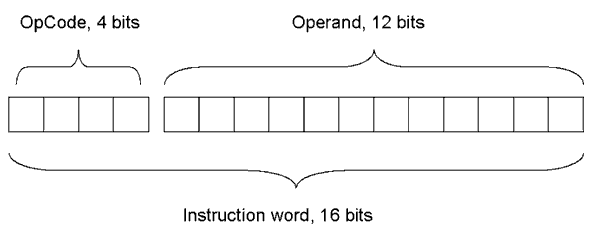
The operand is usually a memory address, so this gives the processor a 12-bit (4 kiloword) address space. I built the memory 16 bits wide so an instruction could be loaded in one piece. In my original design, I planned to have the entire program in 2K of ROM, with 1K of RAM for data storage, and 1K of address space set aside for input and output. The accumulator would be 12 bits wide, and the ALU (arithmetic-logic unit) also 12 bits wide. This was the size of the operand of the immediate load instruction, and was big enough to prove that the computer worked. Later, after I had the processor working, I wanted to load programs into RAM from input. I added 4 bits to the accumulator to allow this (details in main and programming).
After I had decided on the basic architecture of the processor, I drew a detailed plan of the computer that shows all the elements through which the data would move. Here is a diagram of my computer, done in the style of the diagrams developed in the textbook Computer Organization and Design:
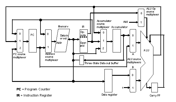
The elements contained in the computer are listed below:
Once the data path had been defined, I could design the control logic. The control logic of the computer is the real heart of the machine. It selects the multiplexor inputs and decides which registers will be written every clock cycle, based on the operation being performed.
Another consideration was the clock speed. The 74LS series gates have about a 10 nanosecond (ns) delay time, and I would probably not have more than 30 gates in any of my logic chains. The slowest part of the machine would be the memory. I used an EPROM with a 250 ns delay. It seemed that a 500 ns cycle time would be enough, but to be safe I started with a 1000 ns cycle (= 1 megahertz clock frequency). After I knew the computer was working, I ran it at 2 MHz, and it worked fine.
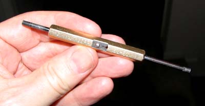
The computer was constructed of 74LS series chips in wire-wrap sockets. (Note: the sockets cost more than the I.C.s!) The connections were made by wire-wrapping, with my trusty hand tool. After wrapping, the connections were checked with a magnifying glass. I only used solder on the power connections, but I probably didn't need to. I tested the outside boards with my test board. I also used a logic probe to debug circuits that weren't working properly.
Once construction was complete I tested it with some simple programs, seen in the programming page. Once I was sure it was working I added a serial port to the memory-input/output board and wrote a short "operating system" (really a program loader). This program allows the user to enter a program as a series of hexidecimal numbers from a terminal. I used both a dumb terminal ($5 at a local flea market) or an old 486 computer running a terminal program. The 486 allows the user to store each program as a text file, and just load it into the computer using a text transfer.
Links to Original CPU pages: