Donn Stewart
13917 Deviar Dr
Centreville, VA 20120
dstew@cpuville.com
13917 Deviar Dr
Centreville, VA 20120
dstew@cpuville.com
The computer has a simple architecture. It has only one programmer-accessible register, the accumulator. Originally 12 bits wide, I added another 4 bits later to allow memory transfers. All load and store operations move data between memory and the accumulator, and the arithmetic-logical instructions use the accumulator as one operand, and data fetched from memory as the other. (The NOT operation, of course, only operates on the accumulator, and the operand in the instruction is ignored.) The results of arithmetic-logical operations are stored in the accumulator. Only the original 12 lower bits of the accumulator can be used for arithmetic-logical operations.
The computer has an instruction word size of 16 bits. The four leftmost bits of an instruction word are the operation code, and the 12 rightmost bits are the operand, like this:
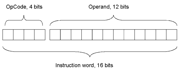
In almost all cases, the operand is a memory address. In the case of the arithmetic-logical instructions the memory address holds the data that is to be operated on together with the data in the accumulator. For the load and store operations, the address is the source or target of the data to be moved. The one exception is the immediate load, LDI. In this case, the 12-bit operand value itself is placed in the accumulator. The various jump instructions use the operand as the target address, except the indirect jump JPI, in which the target address is held in the memory location pointed to by the operand. Here is the instruction set:
| Hex Opcode | Instruction Mnemonic | Operation Performed |
|---|---|---|
| 0 | ADD | Adds contents of memory to accumulator |
| 1 | ADC | Adds contents of memory and carry to accumulator |
| 2 | SUB | Subtracts contents of memory from accumulator |
| 3 | SBC | Subtracts contents of memory and complemented carry from accumulator |
| 4 | AND | Binary AND of memory with accumulator |
| 5 | OR | Binary OR of memory with accumulator |
| 6 | XOR | Binary XOR of memory with accumulator |
| 7 | NOT | Complements accumulator (operand ignored) |
| 8 | LDI | Loads 12-bit value of operand into accumulator (immediate load) |
| 9 | LDM | Loads contents of memory into accumulator |
| A | STM | Stores contents of accumulator to memory |
| B | JMP | Jumps to memory location |
| C | JPI | Jumps to contents of memory location (indirect jump) |
| D | JPZ | If accumulator = zero, jumps to memory location |
| E | JPM | If accumulator is negative (minus), jumps to memory location |
| F | JPC | If carry flag is set, jumps to memory location |
The address space of the computer matches the size of the instruction word operand, 12 bits or 4 kilowords. The memory and input/output ports are addressed in the same way--there are no special input or output instructions. The address space in the computer is laid out this way:
000h to 7FFh (2048 words) Programmable, read-only memory (ROM)
800h to BFFh (1024 words) Static random-access memory (RAM)
C00h to FFFh (1024 ports) Input/output (I/O)
There are 5 input and 5 output ports in the computer, on the memory input/output board. The switch inputs, LED outputs and byte switcher ports are 16 bits wide. The UART ports are eight bits wide. Only the low-order eight bits of the 16 bit accumulator are transferred in UART writes. In UART reads, the upper eight bits of the accumulator are padded with zeros. Here are the computer input and output ports:
| Address | Input | Output |
|---|---|---|
| C00h | DIP switch bank 1 | LED bank 1 |
| C01h | DIP switch bank 2 | LED bank 2 |
| C02h | Byte switcher | Byte switcher |
| C03h | UART data | UART data |
| C04h | UART status | UART control |
The very first program I ran was a simple port reflector:
| Code in ROM | |||||
|---|---|---|---|---|---|
| Label | Location (hex) | Machine Code (hex) | Mnemonic | Operand | Comment |
| Start | 0 00 | 9 C 00 | LDM | Port_0 | Get number from switches |
| 0 01 | A C 00 | STM | Port_0 | Display number on LED's | |
| 0 02 | B 0 00 | JMP | Start | Do it again |
When this program was running, I knew the basic structure of the computer was sound. To further test the machine I wrote the following program. This finds the largest factor of an integer, input from DIP switch bank 1. It is the same program as that first run by the first true computer, the Manchester Mark I "Baby" in 1948. Of course, my instruction set is different than the "Baby's" which had only 7 instructions!
| Code in ROM | |||||
|---|---|---|---|---|---|
| Label | Location (hex) | Machine Code (hex) | Mnemonic | Operand | Comment |
| Start | 0 00 | 9 C 00 | LDM | Port_0 | Get number to factor from input port |
| 0 01 | A 8 00 | STM | Original_number | Store number to factor in memory | |
| 0 02 | A 8 01 | STM | Factor | Starting factor = original number | |
| Loop_1 | 0 03 | 9 8 01 | LDM | Factor | Factor loop |
| 0 04 | 2 0 0F | SUB | One | New factor = old factor - 1 | |
| 0 05 | D 0 0C | JPZ | Quit | If factor = 0, better quit (mistake) | |
| 0 06 | A 8 01 | STM | Factor | Store new factor | |
| 0 07 | 9 8 00 | LDM | Original_number | Test factor by | |
| Loop_2 | 0 08 | 2 8 01 | SUB | Factor | subtracting repeatedly from original number |
| 0 09 | D 0 0C | JPZ | Quit | Factor found-quit | |
| 0 0A | E 0 03 | JPM | Loop_1 | Went past zero, not a factor | |
| 0 0B | B 0 08 | JMP | Loop_2 | Still testing | |
| Quit | 0 0C | 9 8 01 | LDM | Factor | Get the proven factor and |
| 0 0D | A C 00 | STM | Port_0 | Display on the output | |
| 0 0E | B 0 00 | JMP | Start | Start over | |
| One | 0 0F | 0 0 01 | (constant) | ||
| Variables in RAM | |||||
| Label | Location (hex) | ||||
| Original_number | 8 00 | ||||
| Factor | 8 01 |
This program tests an essential subset of the instructions, including the arithmetic instructions and two of the conditional jumps. It also tests the RAM. After this, I decided to write a program loader (see below).
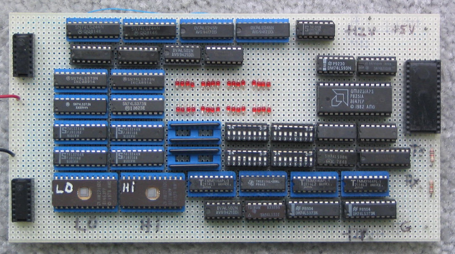
The final configuration of the finished computer allows the computer to receive a program by way of the serial port. The clock speed switch on the logic board is set to 1.8 MHz (position number 7 on). This results in a serial port baud rate of 9600. The input port 1 switches (lower bank) are set to B08Eh, as seen in the picture of the Memory-I/O board. When the computer is started (taken out of reset), it begins execution in ROM at location 000h. There is an instruction there that jumps to the I/O port location and executes whatever instruction it finds there. This feature was put in during the troubleshooting phase of development to allow testing of the computer using a variety of routines stored in ROM. To run a particular test, a jump to that test is put on the port 1 switches. B08Eh is JMP 08Eh. Location 08Eh is the entry point for the program loader (see below).
The computer's serial port is connected to a dumb terminal (or PC running a terminal program) set for 9600 baud, one stop bit, no parity. Power is applied to the computer with the Reset/Run switch in the Reset position. A garbage character may appear on the terminal screen. The programmer may clear the terminal screen if the terminal has this ability. The computer is switched to Run. At this point the computer is ready to take instructions.
This program is the "operating system" of the computer. It takes hex character input from a terminal and converts it to 16-bit instruction words which are loaded into RAM starting at 0x80A. Upon receiving a ctrl-c, it jumps to 0x80A and begins to execute the loaded instructions. It needs upper case characters for A-F. Note that since the character input is 8-bit, and the path through the ALU is 12 bit, there is no easy way to get the highest order nybble of a 16-bit instruction word from the UART into memory. I solved this problem by making a table that contains the high order nybbles. A table entry is selected by the first character of each instruction word, and subsequent characters are converted to binary and placed into the word using the ALU. Later, I built a byte-switcher port which can more directly get low-order data into the high-order accumulator bits, and from there into memory. The instruction table had a gap in it due to the ASCII values of the characters, so I put some constants in the gap to save space.
The instruction set has does not have an instruction for indexed memory access, which is used to access a table. However, indexing can be done indirectly with the following procedure. Two words of RAM are set aside, the first word for the indexed instruction, the second for a return instruction (JPI or JMP). The index value is loaded into the accumulator, and the instruction to be indexed is added (using the ADD instruction). Even though the ALU is only 12 bits wide, the procedure works because the upper 4 bits of the accumulator will always contain the upper 4 bits of the most recently accessed value in memory. The indexed instruction is then placed in the RAM location set aside for it, then a JMP to that location is performed. After the instruction is finished, the return jump is performed. The program loader uses this technique. The base instructions are stored in the table gap in ROM at 0x07C and following, and there are RAM locations set aside for an indexed instruction and following return jump at 0x803 and 0x804.
There is a little patch of code at the end to allow the UART to divide its clock by 16. This helped character flow by improving start bit detection and bit framing. The program code can be entered at 0x027 or 0x08E. The program is in ROM at 0x027 because above it are some small test programs like the port reflector and factor routine. In its finished form, ROM has a JMP 0xC01 at the start. This instruction executes whatever instruction is on the lower DIP switches on the memory I/O board. In the picture, you can see the instruction word B08E there in the switches, which is JMP 08E.
| Label | Location | Contents | Mnemonic | Operand | Comment |
|---|---|---|---|---|---|
| ROM: | |||||
| 027 | 907C | LDM | BRetInst | Base Return Inst (JPI RetAdd1) | |
| 028 | A804 | STM | RetInst | ||
| 029 | 804D | LDI | 04D | UART mode with undivided clk | |
| 02A | AC04 | STM | UART Control | ||
| 02B | 8037 | LDI | 037 | UART command instruction | |
| 02C | AC04 | STM | UART Control | ||
| 02D | 8FFF | LDI | FFF | Initial instruction index (-1) | |
| 02E | A807 | STM | InstIndex | ||
| MainLoop | 02F | 8004 | LDI | 004 | Initial Nybble no. (loop 4 times) |
| 030 | A809 | STM | NybbleNo | ||
| ReturnLoop | 031 | 9809 | LDM | NybbleNo | |
| 032 | 2079 | SUB | One | ||
| 033 | E03F | JPM | Done | Instruction complete; store in RAM | |
| 034 | A809 | STM | NybbleNo | Instruction not complete; | |
| 035 | 007D | ADD | BLDMMask | Get nybble mask by creating indexed | |
| 036 | A803 | STM | IndInst | instruction | |
| 037 | 803A | LDI | 03A | ||
| 038 | A805 | STM | RetAdd1 | ||
| 039 | B803 | JMP | IndInst | Jump to indexed instruction | |
| 03A | A808 | STM | Mask | Store mask retrieved from table | |
| 03B | 803E | LDI | 03E | ||
| 03C | A806 | STM | RetAdd2 | Store return address | |
| 03D | B04E | JMP | RxPoll_1 | Get next char and process | |
| 03E | B031 | JMP | ReturnLoop | ||
| Done | 03F | 9807 | LDM | InstIndex | Increment index and store |
| 040 | 0079 | ADD | One | ||
| 041 | A807 | STM | InstIndex | ||
| 042 | 007E | ADD | BSTMInst | Create indexed store instruction | |
| 043 | A803 | STM | IndInst | ||
| 044 | 8048 | LDI | 048 | Return address | |
| 045 | A805 | STM | RetAdd1 | ||
| 046 | 9802 | LDM | Inst | ||
| 047 | B803 | JMP | IndInst | Store instruction in RAM | |
| TxLoop_2 | 048 | 9C04 | LDM | UART Control | |
| 049 | 4079 | AND | One | Check TxRdy | |
| 04A | D048 | JPZ | TxLoop_2 | ||
| 04B | 800D | LDI | ASCII CR | Carriage return | |
| 04C | AC03 | STM | UART Data | Send CR to display | |
| 04D | B02F | JMP | MainLoop | ||
| RxPoll_1 | 04E | 9C04 | LDM | UART Control | |
| 04F | 407A | AND | Two | Check RxRdy | |
| 050 | D04E | JPZ | RxPoll_1 | ||
| 051 | 9C03 | LDM | UART Data | Get Char | |
| 052 | A800 | STM | Char | Store char | |
| 053 | 206B | SUB | CTRL-C | End of input? | |
| 054 | D80A | JPZ | ProgStart | Yes-start program | |
| TxPoll_1 | 055 | 9C04 | LDM | UART Control | No- Echo Char and process |
| 056 | 4079 | AND | One | Check TxRdy | |
| 057 | D055 | JPZ | TxPoll_1 | ||
| 058 | 9800 | LDM | Char | ||
| 059 | AC03 | STM | UART Data | Echo Character | |
| 05A | 207B | SUB | 30hex | Make index by subtracting 30h | |
| 05B | 007F | ADD | BLDMInst | Create indexed LDM instruction | |
| 05C | A803 | STM | IndInst | Store in RAM | |
| 05D | 8060 | LDI | 060 | Return address | |
| 05E | A805 | STM | RetAdd1 | ||
| 05F | B803 | JMP | IndInst | Get partial inst from table | |
| 060 | A801 | STM | PartInst | ||
| 061 | 9808 | LDM | Mask | ||
| 062 | D067 | JPZ | Next1 | Special for highest nybble | |
| 063 | 4801 | AND | PartInst | Mask off partial inst | |
| 064 | 0802 | ADD | Inst | Combine with prior inst and store | |
| 065 | A802 | STM | Inst | ||
| 066 | C806 | JPI | RetAdd2 | Done | |
| Next1 | 067 | 4801 | AND | PartInst | Mask off partial inst |
| 068 | A802 | STM | Inst | Store (high nybble) | |
| 069 | C806 | JPI | RetAdd2 | Done | |
| Zero | 06A | 0000 | |||
| CTRL-C | 06B | 0003 | |||
| MaskTable | 06C | 000F | |||
| 06D | 00F0 | ||||
| 06E | 0F00 | ||||
| InstTable | 06F | 0000 | |||
| 070 | 1111 | ||||
| 071 | 2222 | ||||
| 072 | 3333 | ||||
| 073 | 4444 | ||||
| 074 | 5555 | ||||
| 075 | 6666 | ||||
| 076 | 7777 | ||||
| 077 | 8888 | ||||
| 078 | 9999 | ||||
| One | 079 | 0001 | |||
| Two | 07A | 0002 | |||
| 30hex | 07B | 0030 | |||
| BRetInst | 07C | C805 | JPI | RetAdd1 | |
| BLDMMask | 07D | 906C | LDM | MaskTable | |
| BSTMInst | 07E | A80A | STM | ProgStart | |
| BLDMInst | 07F | 906F | LDM | InstTable | |
| 080 | AAAA | ||||
| 081 | BBBB | ||||
| 082 | CCCC | ||||
| 083 | DDDD | ||||
| 084 | EEEE | ||||
| 085 | FFFF | ||||
| 08E | 907C | LDM | BRetInst | ||
| 08F | A804 | STM | RetInst | ||
| 090 | 804E | LDI | 04E | UART mode with Rx and Tx clk/16 | |
| 091 | AC04 | STM | UART Control | ||
| 092 | B02B | JMP | 02B | Entry with UART clk/16 | |
| Label | Location | Contents | Mnemonic | Operand | Comment |
| RAM: | |||||
| Char | 800 | ||||
| PartInst | 801 | ||||
| Inst | 802 | ||||
| IndInst | 803 | ||||
| RetInst | 804 | ||||
| RetAdd1 | 805 | ||||
| RetAdd2 | 806 | ||||
| InstIndex | 807 | ||||
| Mask | 808 | ||||
| NybbleNo | 809 | ||||
| ProgStart | 80A |
Links to Original CPU pages: