Donn Stewart
13917 Deviar Dr
Centreville, VA 20120
dstew@cpuville.com
13917 Deviar Dr
Centreville, VA 20120
dstew@cpuville.com
The data path diagrams on the overall design page, and the data path design page, leave out some crucial details: the control lines for the multiplexors, the register clock pulse lines, and the system control lines, such as read, write, memory request, and input-output request. These lines come from the control logic. It is the task of the processor control logic to interpret the machine language instructions of the computer program, and set system control lines to read or write memory or ports, set the multiplexor control lines to direct the data through the processor data path to appropriate targets, and at the end of a clock cycle, to send clock pulses to any registers in the data path that need to be written. For example, if we are fetching an opcode from the memory, the control logic must assert the memory request and read system control lines, and the address source multiplexor in the data path must be set to 1, sending the address from the program counter to the memory. The memory will put the data onto the data bus, and at the end of the clock cycle, the control logic must send a clock pulse to the opcode portion of the instruction register. In essence, the control logic is the real computer, and the data path, system, and ALU are its servants.
How does the control logic do this? At the heart of the control logic is a "finite state machine" that is the real heart of this or any computer. A finite state machine is both a theoretical and actual machine that does what we call "computing". The finite state machine is a derivation of a universal computing machine conceived by mathematician Alan Turing in 1936 as a way to define what is or is not "computable". The finite state machine differs from a Turing machine in that the number of states is finite, where in the Turing machine the number of states is infinite.
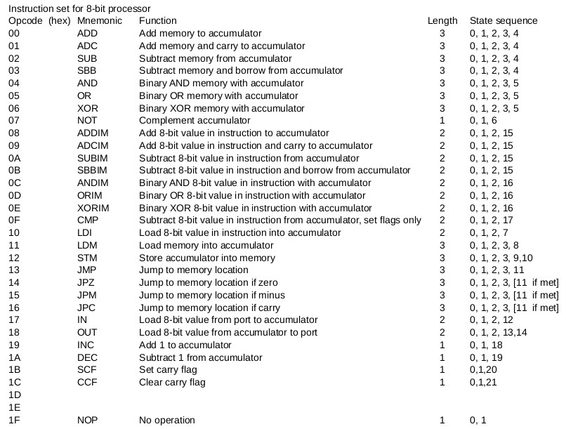
The "states" of the finite state machine in a computer correspond to the steps performed in a computation. In the 8-bit computer described here, each step is done in one clock cycle. In the instruction set for this machine, each machine language instruction is performed by two to six states, as shown here:
The task of designing the control logic falls into two parts. First, for a given instruction, the control logic needs to produce the correct series of states, one for each clock cycle. Second, for each state, the control logic needs to set the system and data path control lines, and produce the proper register write clock pulses at the end of the cycle.
The first task, producing the state sequence for a given instruction, is done by the finite state machine. The finite state machine here is built using a register, which holds the current state, and a combinatorial logic circuit that produces the next state. This combinatorial logic circuit takes as its input the current state, the current instruction, and in this processor the zero, carry and minus flags. These flags are used to alter the sequence of states for the conditional jump instructions. At the end of the clock cycle, on the rising edge of the clock, the next state is written into the state register, to become the current state.
The second task, setting the system and data path control lines, and creating the register write pulses, is done by a logic network and some additional registers and delay circuits to produce the proper timing for system controls. The input to this system is the current state. All of the controls and pulses are determined by the current state alone in this design.
The details of the next-state logic for the finite state machine are here.
The details of the control signals logic are here
8-bit processor links: